
In this article I’ll try to show how to use an MSP430 with a DAC7564. This is probably the first from a series of articles showing different devices I plan to use in a project.
The DAC7564
The DAC7564 is a low-power, voltage-output, four-channel, 12-bit digital-to-analog converter (DAC). The device includes a 2.5V, 2ppm/°C internal reference. The device is monotonic, provides very good linearity, and minimizes undesired code-to-code transient voltages (glitch). A DAC is said to be monotonic if the output either increases or remains constant for increasing digital inputs such that the output will always be a nondecreasing function of input. The DAC7564 architecture consists of a string DAC followed by an output buffer amplifier. An N-bit string DAC simply consists of 2N equal resistors in series and 2N switches (usually CMOS), one between each node of the chain and the output. The output is taken from the appropriate tap by closing just one of the switches. The string DAC is inherently monotonic—even if a resistor is accidentally short-circuited, output n cannot exceed output n + 1.
Linearity error of a converter is a deviation of the analog values, in a plot of the measured conversion relationship, from a straight line. The string DAC it is lineal if all the resistors are equal.
A glitch is a switching transient appearing in the output during a code transition. The worstcase DAC glitch (in R-2R) generally occurs when the DAC is switched between the 011…111 and 100…000 codes. In sting DACs only two switches operate during a transition, resulting in a low-glitch architecture Also, the switching glitch is not code-dependent.
The DAC7564 uses a versatile 3-wire serial interface that operates at clock rates up to 50MHz. The interface is compatible with standard SPI, QSPI, Microwire, and digital signal processor (DSP) interfaces.
The DAC7564 input shift register is 24 bits wide. Bits DB23 to DB16 are used for control and configuration and bits DB15 to DB4 for data. Bits DB0, DB1, DB2, and DB3 are ignored by the DAC. All 24 bits of data are loaded into the DAC under the control of the serial clock input, SCLK.
The DAC7564 receives all 24 bits of data and decodes the first eight bits in order to determine the DAC operating/control mode. The 12 bits of data that follow are decoded by the DAC to determine the equivalent analog output.
The write sequence begins by bringing the SYNC line low. Data from the DIN line are clocked into the 24-bit bits wide shift register on each falling edge of SCLK. After receiving the 24th falling clock edge, the DAC7564 decodes the eight control bits and 12 data bits to perform the required function, without waiting for a SYNC rising edge. A new write sequence starts at the next falling edge of SYNC.
Data Input Register Format
The first two control bits (DB23 and DB22) are the address match bits. The DAC7564 offers hardware-enabled addressing capability, allowing a single host to talk to up to four DAC7564s through a single SPI bus without any glue logic, enabling up to 16-channel operation. The state of DB23 should match the state of pin A1; similarly, the state of DB22 should match the state of pin A0. If there is no match, the control command and the data (DB21…DB0) are ignored by the DAC7564. That is, if there is no match, the DAC7564 is not addressed. Both pins are connected to ground therefore those bits are 0.
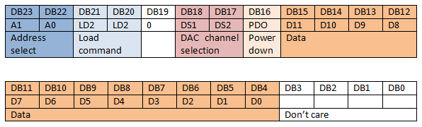
Data Input Register
LD1 (DB21) and LD0 (DB20) control the loading of each analog output with the specified 12-bit data value or power-down command. In the final setup the DAC will need to update each channel individually and at different times so Single-channel update will be used which implies having DB21 = 0 and DB20 = 1. The final control bit, PD0 (DB16), selects the power-down mode of the DAC7564 channels as well as the power-down mode of the internal reference. In this application there is no concern over power savings so bit SB16 will be 0.
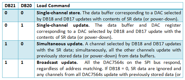
Load commands
Bit DB19 must always be ‘0’.The DAC channel select bits (DB18, DB17) control the destination of the data (or power-down command) from DAC A through DAC D.
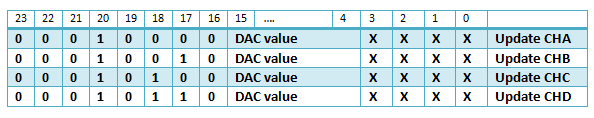
The final control matrix to be used is as follow;
The initial test are done using the internal voltage reference enabled by default. The DAC7564 includes a 2.5V internal reference with 0.004% Initial Accuracy (typ) and 5ppm/°C Temperature Drift (max). In the future a 4.096 V reference will be used and for that the internal reference need to be disabled. To do that a serial command that requires a 24-bit write sequence must be used.
The software
An MSP430 is used to send the data and the SPI communication is done by bit-banging. A library provides functions to send, receive and transfer data using SPI protocol. Being a bit-bang communication there is no particular hardware module necessary and any MSP430 would work, in this particular case a MSP430F2274 is used. The function send 8 bit at a time and the data needs to be rearranged before sending. The first byte (DB23…DB16) corresponds to the address, the load command, power down bit and the channel selection. The second byte (DB15…D8) corresponds to the eight most significant bits of the 12 bits DAC value. In the third and last byte the remaining 4 bits of the DAC value is sent. The image below shows a capture of the data pattern made using a logic analyzer.

Testing
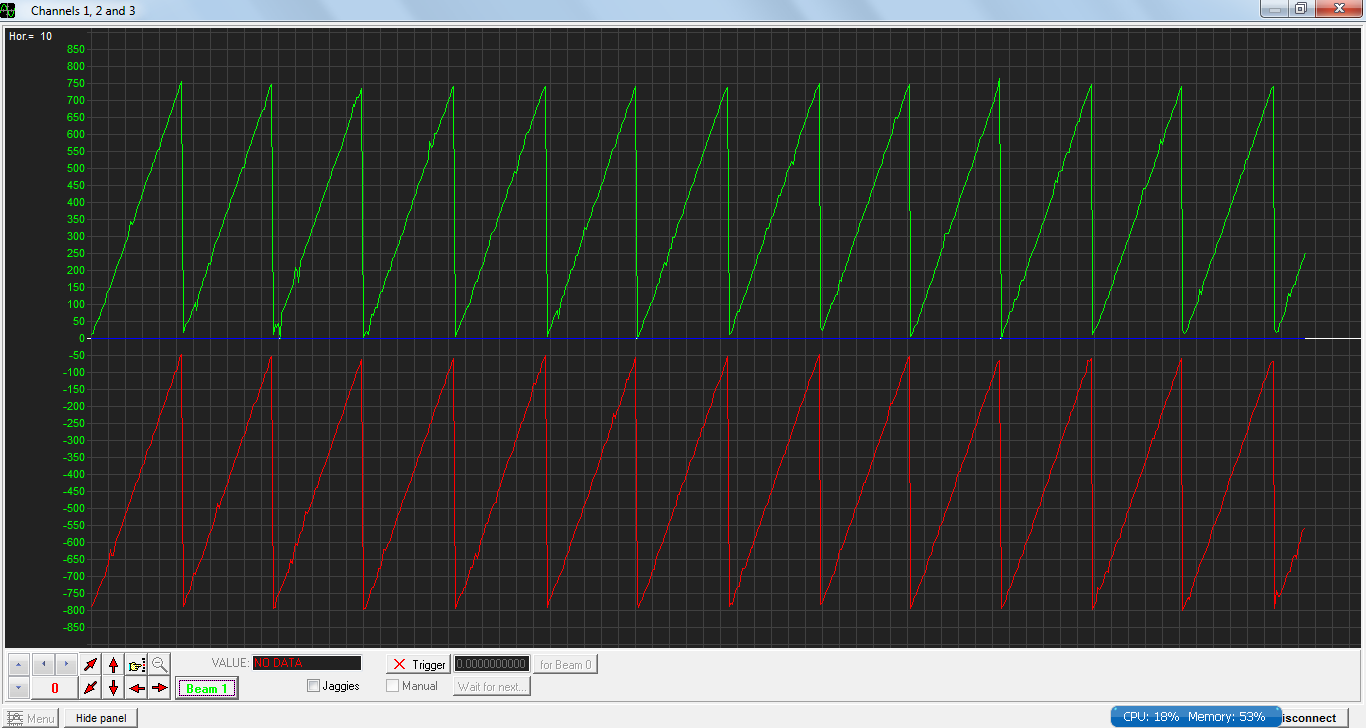
A Launchpad was used as an oscilloscope to see the DAC’s outputs (I don’t have a scope, I’m saving for one. If you have found the site useful, please consider making a donation and help me buy one 🙂). For the test the internal 2.5 V voltage reference was used and the microcontroller generated a ramp style signal and a couple of sine waves. The picture shows the DAC’s outputs (sampled at 55[Hz]).
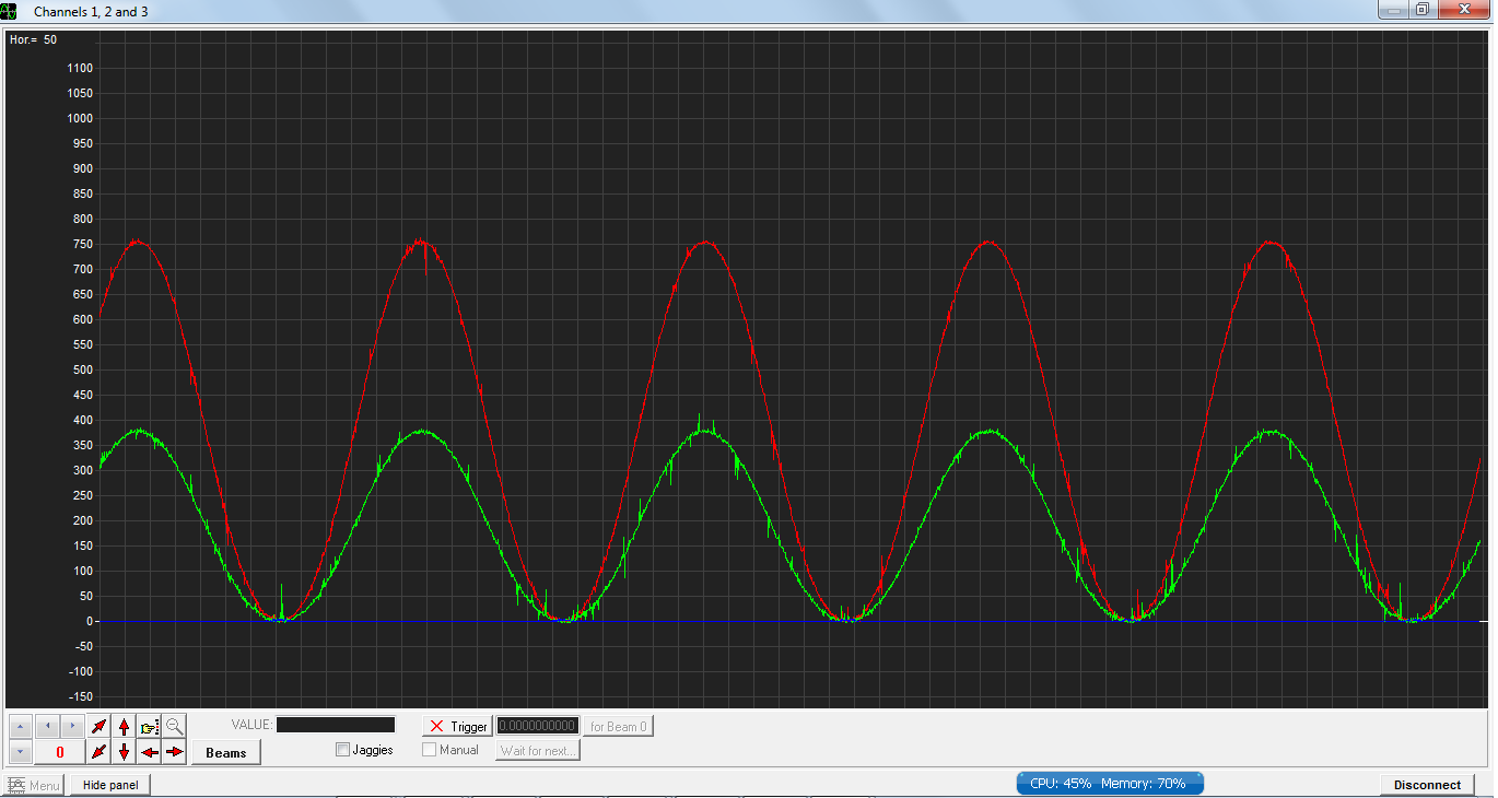
The sine waves are generated using a 256 points look-up table. For the green one the value from the table is divided by two.
References
The data conversion handbook. Analog Devices Series Electronics & Electrical. Walter Allan Kester. 3 Ed. Newnes, 2005.

Pingback: Interfacing the DAC7564 to an MSP430 • Tech Projects