Digital to Analog Converters are essential to the electronics market. They are used in almost every piece of electronic equipment which involves interaction with an external world. Whether it be mere LED blinking (LED dimming) or complex voice translators, DACs are important. DAC7715 provides a four-channel output and takes 12-bit serial input. It has a good resolution of 12-bits and can sink up to 5 mA of current. It contains a selectable Reset that combined with asynchronous clear registers and set them to either zero-scale or midscale. For protection purposes, it has an ESD protection circuit.
The article is an introduction to DAC7715, working, specifications and applications.
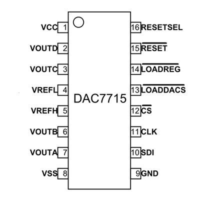
DAC7715 Pinout
The pinout of the DAC7715 Digital to Analog Converter IC is shown below:

Pin Configuration
DAC7715 is available in the SOIC package. This DAC has a total of 16 pins. The pin configuration detail in tabular is mentioned below:
| Pin Number | Pin Name | Function |
|---|---|---|
| 1 | VCC | Positive Power Supply pin. We can power this DAC module either with a single 15V power supply or a +15V and -15V dual power supply. |
| 2 | VOUTD | Analog Output Voltage D pin |
| 3 | VOUTC | Analog Output Voltage C pin |
| 4 | VREFL | Low Reference Voltage Input pin It gives out minimum output voltage |
| 5 | VREFH | High Reference Voltage Input pin It gives out maximum output voltage |
| 6 | VOUTB | Analog Output Voltage B pin |
| 7 | VOUTA | Analog Output Voltage A pin |
| 8 | VSS | Negative Power Supply pin |
| 9 | GND | Ground pin |
| 10 | SDI | Serial Data Input pin |
| 11 | CLK | Serial Clock input pin |
| 12 | CS | Chip Select Input pin |
| 13 | LOADDACS | DAC register state pin In HIGH state, registers become latched and transparent in LOW state. |
| 14 | LOADREG | Selective Input register state pin In LOW state, registers become transparent and latched in HIGH state. |
| 15 | RESET | Asynchronous Reset Input pin At LOW state, it will set to zero-state or mid-state. |
| 16 | RESETSEL | Code Reset Select pin When LOW, DAC sets to 000H. In HIGH state, DAC sets to 800H. |
DAC7715 Features and Specifications
- Number of Output Channels: 4
- Power Consumption: 250 mW
- Operating Temperature Range: -400C – 850C
- DAC Resolution: 12-bits
- DAC Settling Time: 10 usec to 0.012%
- VCC to VSS Range: -0.3Volts – 32Volts
- VCC to GND Range: -0.3Volts – 16Volts
- VSS to GND Range: 0.3Volts to -16Volts
- Output Current Range: -5 mA to 5 mA
- Maximum High Reference Voltage: 10 Volts
- Maximum Low Reference Voltage: -10 Volts
- Operational Frequency: 10 kHz
- Package Type: SOIC-16 package
- All the data inputs of DAC are double-buffered.
- The DAC can either work on single supply i.e. 15 Volts or dual supply i.e +15 Volts and -15 Volts.
- The chipset is embedded with electrostatic discharge protection incase of malfunctioning.
Alternate Options
- DAC8814
- DAC8811
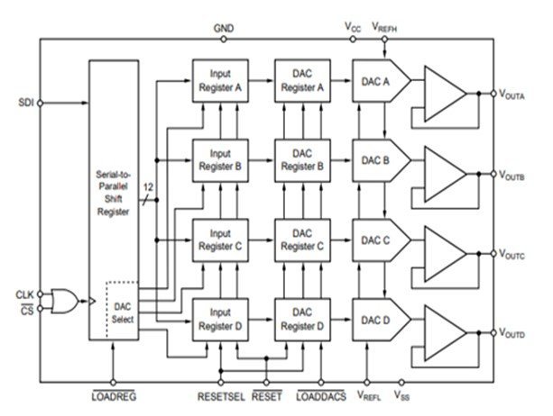
Block Diagram
The digital to analog converter has 4 output channels. The block diagram of the internal circuitry to have the know-how of components is provided below:
How does DAC7715 DAC work?
The Digital to Analog converter takes in the digital binary signals, processes them, and then outputs continuous analog signals. This is done with the help of an Inter-Integrated Circuit(I2C) interface. The binary data is transferred serially to the DAC converter through SDI and SCL gives the clock. After complete reception, all binary 0s are mapped as the lowest voltage while all binary 1s are mapped to maximum positive and negative voltage respectively. The coming section will describe the application of DAC7715.
Example Circuit DAC7715
The sample example circuit diagram of the dual supply digital to analog converter is given below:
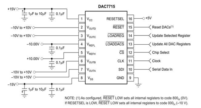
This is a bi-operational analog voltage supply circuit. The chip is powered with 15 volts power supply. The digital data is received by the device through a Serial Data Input pin and Clock through SCL. As it is a dual supply circuit, both reference pins are given some volts according to technical specifications. Here VREFH is connected to +10 Volts and VREFL is connected to -10 Volts. This will limit the outputs between VREFL and VREFH. After the complete transfer of 12-bit serial data, LOADADCS is updated and conversion takes place. The resultant analog signals then received at the four output pins is between -10 to +10 Volts and supplied to the load.
Applications
- Consumer electronics
- Smartphones
- Data Logging Systems
- Process Control
- Video Signals
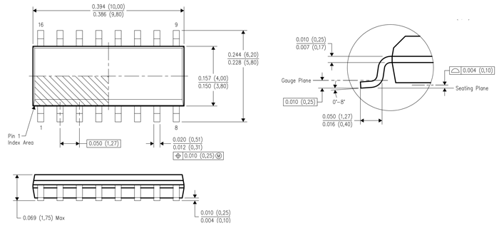
2D Diagram
Related DAC Modules: